US 11,901,371 B2
Contact structure and display device including the same
YounSub Kim, Seongnam-si (KR); JongSik Shim, Paju-si (KR); ByeongUk Gang, Paju-si (KR); and SeongHwan Hwang, Seoul (KR)
Assigned to LG DISPLAY CO., LTD., Seoul (KR)
Filed by LG DISPLAY CO., LTD., Seoul (KR)
Filed on Sep. 26, 2022, as Appl. No. 17/952,419.
Application 17/952,419 is a division of application No. 17/200,531, filed on Mar. 12, 2021, granted, now 11,488,986.
Application 17/200,531 is a division of application No. 16/165,059, filed on Oct. 19, 2018, granted, now 10,985,189, issued on Apr. 20, 2021.
Claims priority of application No. 10-2017-0169193 (KR), filed on Dec. 11, 2017.
Prior Publication US 2023/0018904 A1, Jan. 19, 2023
Int. Cl. H01L 27/12 (2006.01); H01L 23/522 (2006.01); H01L 23/528 (2006.01); G02F 1/13 (2006.01)
CPC H01L 27/124 (2013.01) [G02F 1/13 (2013.01); H01L 23/5226 (2013.01); H01L 23/528 (2013.01)] 5 Claims
OG exemplary drawing
 
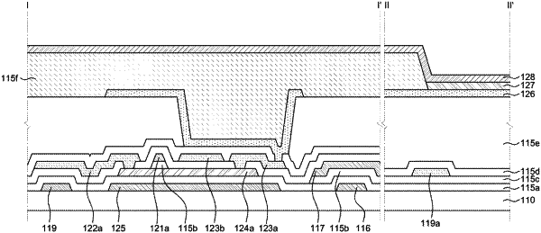
1. A contact structure for a display device, comprising:
a lower layer;
a first insulating layer disposed on the lower layer and having a contact hole to expose a part of the lower layer;
an upper layer disposed on the first insulating layer contacting the lower layer through the contact hole; and
a second insulating layer disposed below the lower layer,
wherein the lower layer is formed of a semiconductor and the upper layer is formed of a conductive material,
wherein the contact hole exposes a part of an upper surface of the lower layer, a side of the lower layer and a part of an upper surface of the second insulating layer.