| CPC H01L 27/1218 (2013.01) [G02F 1/1368 (2013.01); G02F 1/136209 (2013.01); G02F 1/136222 (2021.01); H01L 27/127 (2013.01); H01L 27/1288 (2013.01)] | 8 Claims |
|
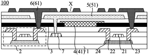
1. A method of manufacturing an array substrate, the method comprising:
providing a substrate, the substrate having a display area and a bezel area;
forming a gate conductive layer on a side of the substrate, the gate conductive layer including gates of a plurality of thin film transistors and at least one first alignment mark located in the bezel area;
forming a source-drain conductive thin film on a side of the gate conductive layer away from the substrate;
aligning a first mask and the substrate on which the gate conductive layer and the source-drain conductive thin film have been formed according to the at least one first alignment mark;
patterning the source-drain conductive thin film by using the first mask as a shield to form sources and drains of the plurality of thin film transistors and at least one second alignment mark located in the bezel area, so as to obtain a source-drain conductive layer, wherein a reflectivity of the source-drain conductive layer is greater than a reflectivity of the gate conductive layer;
forming a black matrix thin film on a side of the source-drain conductive layer away from the substrate;
aligning a second mask and the substrate on which the gate conductive layer, the source-drain conductive layer and the black matrix thin film have been formed according to the at least one second alignment mark;
patterning the black matrix thin film by using the second mask as a shield to form a black matrix, wherein orthographic projections of the plurality of thin film transistors on the substrate are located within an orthographic projection of the black matrix on the substrate; and
forming a color filter layer on the substrate on which the black matrix has been formed.
|