| CPC H01L 27/1207 (2013.01) [H01L 21/8221 (2013.01); H01L 21/823412 (2013.01); H01L 21/823418 (2013.01)] | 20 Claims |
|
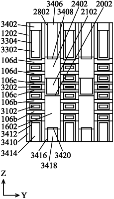
1. A semiconductor device structure, comprising:
a first plurality of semiconductor layers disposed at a first location of the semiconductor device structure, wherein the first plurality of semiconductor layers comprises a first group of semiconductor layers, a second group of semiconductor layers disposed over and aligned with the first group of semiconductor layers, and a third group of semiconductor layers disposed over and aligned with the second group of semiconductor layers;
a first source/drain epitaxial feature in contact with a first number of semiconductor layers of the first group of semiconductor layers, wherein the first source/drain epitaxial feature has a first height;
a first dielectric material disposed over the first source/drain epitaxial feature;
a second source/drain epitaxial feature in contact with a second number of semiconductor layers of the third group of semiconductor layers, wherein the second source/drain epitaxial feature is disposed over the first dielectric material;
a second plurality of semiconductor layers disposed at a second location of the semiconductor device structure, wherein the second plurality of semiconductor layers comprises a fourth group of semiconductor layers, a fifth group of semiconductor layers disposed over and aligned with the fourth group of semiconductor layers, and a sixth group of semiconductor layers disposed over and aligned with the fifth group of semiconductor layers;
a third source/drain epitaxial feature in contact with a third number of semiconductor layers of the fourth group of semiconductor layers, wherein the third source/drain epitaxial feature has a second height different from the first height;
a second dielectric material disposed over the third source/drain epitaxial feature; and
a fourth source/drain epitaxial feature in contact with a fourth number of semiconductor layers of the sixth group of semiconductor layers, wherein the fourth source/drain epitaxial feature is disposed over the second dielectric material.
|