| CPC H01L 27/0924 (2013.01) [H01L 21/0228 (2013.01); H01L 29/0665 (2013.01); H01L 29/66795 (2013.01); H01L 29/7851 (2013.01)] | 20 Claims |
|
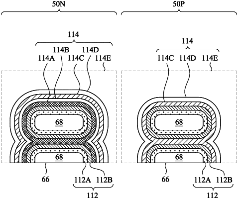
1. A device comprising:
first nanostructures;
a gate dielectric on the first nanostructures; and
a first gate electrode comprising:
a first layer on the gate dielectric, the first layer comprising an n-type work function metal, the first layer being disposed in an area between the first nanostructures;
a second layer on the first layer, the second layer comprising a barrier material, the barrier material being different from the n-type work function metal, the area between the first nanostructures being free of the second layer; and
a third layer on the second layer, the third layer comprising a p-type work function metal, the p-type work function metal being different from the n-type work function metal, the p-type work function metal being different from the barrier material.
|