| CPC H01L 27/092 (2013.01) [H01L 21/32139 (2013.01); H01L 21/76895 (2013.01); H01L 21/8221 (2013.01); H01L 21/823828 (2013.01); H01L 21/823871 (2013.01); H01L 23/528 (2013.01); H01L 23/535 (2013.01); H01L 27/0207 (2013.01); H01L 29/0847 (2013.01); H01L 29/1033 (2013.01); H01L 29/41758 (2013.01); H01L 29/42376 (2013.01); H03K 19/0948 (2013.01)] | 10 Claims |
|
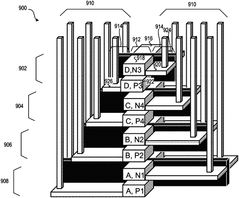
1. A method of forming a semiconductor device, comprising:
forming a plurality of transistor pairs that are stacked over a substrate, wherein the plurality of transistor pairs have a plurality of gate electrodes that are stacked over the substrate and electrically coupled to gate structures of the plurality of transistor pairs, and a plurality of source/drain (S/D) local interconnects that are stacked over the substrate and electrically coupled to source regions and drain regions of the plurality of transistor pairs, wherein each of the plurality of transistor pairs comprises a n-type transistor and a p-type transistor that are stacked over one another; and
performing a sequence of vertical and lateral etch steps to etch the plurality of the gate electrodes and the plurality of S/D local interconnects so that the plurality of the gate electrodes and the plurality of S/D local interconnects have a staircase configuration.
|