| CPC H01L 27/0886 (2013.01) [H01L 21/823418 (2013.01); H01L 21/823431 (2013.01); H01L 21/823437 (2013.01); H01L 21/823475 (2013.01); H01L 21/823481 (2013.01); H01L 27/0207 (2013.01); H01L 29/66545 (2013.01); H10B 10/12 (2023.02)] | 20 Claims |

|
1. A method of manufacturing a semiconductor device, the method comprising:
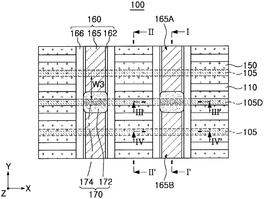
forming active regions extending in a first direction on a substrate by removing a portion of the substrate;
forming a dummy active region by removing an upper portion of a first active region among the active regions;
forming a second gate separation layer on the dummy active region;
forming a sacrificial structure extending in a second direction crossing the first direction, on the active regions and the second gate separation layer;
removing a portion of the second gate separation layer from outside of the sacrificial structure;
forming source/drain regions on the active regions, at both sides of the sacrificial structure;
forming an interlayer insulating layer covering the source/drain regions;
removing the sacrificial structure and forming a gate structure in a region in which the sacrificial structure is removed;
forming an opening by removing a portion of the gate structure to expose the second gate separation layer; and
forming a first gate separation layer by filling the opening with an insulating material.
|