| CPC H01L 27/0688 (2013.01) [H01L 23/481 (2013.01); H10B 41/60 (2023.02); H10B 43/20 (2023.02); H10B 63/30 (2023.02); H10B 63/84 (2023.02)] | 16 Claims |
|
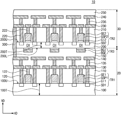
1. A three-dimensional semiconductor device, comprising:
a lower substrate;
a plurality of lower transistors disposed on the lower substrate;
an upper substrate disposed on the lower transistors;
a plurality of lower conductive lines disposed between the lower transistors and the upper substrate;
a plurality of upper transistors disposed on a top surface of the upper substrate;
a plurality of upper conductive lines disposed on the upper transistors;
an upper penetration via penetrating the upper substrate; and
a plurality of intermediate transistors disposed on a bottom surface of the upper substrate,
wherein at least one of the lower transistors is connected to a corresponding one of the lower conductive lines, and at least one of the upper transistors is connected to a corresponding one of the upper conductive lines,
wherein each of the upper transistors comprises:
an upper gate electrode disposed on the top surface of the upper substrate;
a first upper source/drain pattern disposed in the upper substrate at a first side of the upper gate electrode; and
a second upper source/drain pattern disposed in the upper substrate at a second, opposing side of the upper gate electrode,
wherein each of the lower transistors comprises:
a lower gate electrode disposed on the lower substrate;
a first lower source/drain pattern disposed in the lower substrate at a first side of the lower gate electrode; and
a second lower source/drain pattern disposed in the lower substrate at a second, opposing side of the lower gate electrode,
wherein the upper gate electrode comprises polycrystalline silicon germanium (SiGe), and the lower gate electrode comprises polycrystalline silicon or polycrystalline germanium,
wherein one terminal of the at least one of the lower transistors is electrically connected to one terminal of the at least one of the upper transistors through corresponding ones of the lower conductive lines, the upper penetration via and corresponding ones of the upper conductive lines,
wherein the upper penetration via extends above the upper substrate and is disposed adjacent to the upper gate electrode of at least one of the upper transistors above the upper substrate,
wherein each of the plurality of intermediate transistors comprises:
a back-gate electrode disposed on the bottom surface of the upper substrate; and
a back-gate insulating layer interposed between the upper substrate and the back-gate electrode.
|