| CPC H01L 27/0251 (2013.01) [H01L 27/124 (2013.01); H01L 27/1255 (2013.01); H01L 27/1259 (2013.01)] | 15 Claims |
|
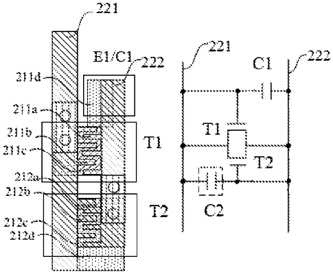
1. An array substrate, comprising a plurality of conductive lines and an electrostatic protection circuit on a base substrate, two of the plurality of conductive lines being connected to the electrostatic protection circuit, and the two of the plurality of conductive lines connected to the electrostatic protection circuit being a first conductive line and a second conductive line, respectively,
wherein the electrostatic protection circuit comprises a first transistor, a second transistor, and a first capacitor,
a first electrode of the first transistor, a first electrode of the second transistor and a gate electrode of the second transistor are connected to the second conductive line, and a second electrode of the first transistor, a second electrode of the second transistor and a gate electrode of the first transistor are connected to the first conductive line, and
one terminal of the first capacitor is connected to the gate electrode of the first transistor and the other terminal of the first capacitor is connected to the second conductive line,
the first electrode of the first transistor is an interdigital electrode comprising a plurality of first fingers directly contact with the second conductive line, the second electrode of the first transistor is an interdigital electrode comprising a plurality of second fingers directly contact with the first conductive line, and an orthographic projection of the gate electrode of the first transistor on the base substrate overlaps both of orthographic projections of the plurality of first fingers on the base substrate and orthographic projections of the plurality of second fingers on the base substrate,
the first electrode of the second transistor is an interdigital electrode comprising a plurality of third fingers directly contact with the second conductive line, the second electrode of the second transistor is an interdigital electrode comprising a plurality of fourth fingers directly contact with the first conductive line, and an orthographic projection of the gate electrode of the second transistor on the base substrate overlaps both of orthographic projections of the plurality of third fingers on the base substrate and orthographic projections of the plurality of fourth fingers on the base substrate.
|