| CPC H01L 25/18 (2013.01) [H01L 21/78 (2013.01); H01L 23/5386 (2013.01); H01L 24/16 (2013.01); H01L 24/73 (2013.01); H01L 24/94 (2013.01); H01L 25/50 (2013.01); H01L 2224/16225 (2013.01); H01L 2224/73204 (2013.01)] | 20 Claims |
|
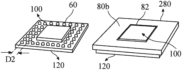
1. A method for forming a semiconductor package, comprising:
bonding a plurality of first integrated circuit dies onto a wafer having a plurality of second integrated circuit dies formed thereon, by directly contacting a first interconnect structure of each first integrated circuit die with an interconnect structure of the corresponding second integrated circuit die such that a metal portion of the first interconnect structure and a metal portion of the interconnect structure are in direct contact and a dielectric portion of the first interconnect structure and a dielectric portion of the interconnect structure are in direct contact, followed by heating the first and second integrated circuit dies to a temperature so that the metal portion of the first interconnect structure and the metal portion of the interconnect structure are interconnected by metal inter-diffusion;
cutting the wafer into individual pieces each having at least one first integrated circuit die bonded to the second integrated circuit die;
bonding an individual piece of the wafer to a first side of a substrate so that the first integrated circuit die is being surrounded by a portion of the substrate; and
bonding a second side of the substrate to a printed circuit board, wherein the first integrated circuit die is exposed to a gap defined by the second integrated circuit die, the substrate, and the printed circuit board, and the substrate has an opening extending through the entire thickness of the substrate, wherein the opening is sized to allow the circumference of the first integrated circuit die in the opening.
|