| CPC H01L 25/0753 (2013.01) [H01L 21/187 (2013.01); H01L 21/2007 (2013.01); H01L 21/447 (2013.01); H01L 23/49513 (2013.01); H01L 24/04 (2013.01); H01L 24/06 (2013.01); H01L 24/83 (2013.01); H01L 24/94 (2013.01); H01L 24/97 (2013.01); H01L 33/0066 (2013.01); H01L 33/0093 (2020.05); H01L 33/0095 (2013.01); H01L 33/486 (2013.01); H01L 33/62 (2013.01); H01L 24/32 (2013.01); H01L 2224/32225 (2013.01); H01L 2224/32245 (2013.01); H01L 2224/83001 (2013.01); H01L 2224/83005 (2013.01); H01L 2224/8314 (2013.01); H01L 2224/83121 (2013.01); H01L 2224/83193 (2013.01); H01L 2924/12041 (2013.01); H01L 2924/12042 (2013.01)] | 19 Claims |

|
10. A semiconductor device, comprising:
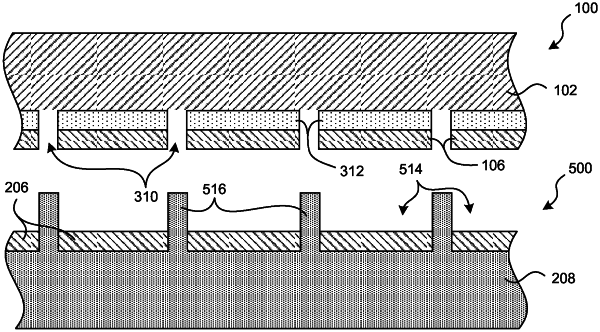
a silicon substrate having a front surface and a back surface opposite the front surface, wherein the front surface includes a recess defined by a bottom surface situated between the front surface and the back surface and by sidewalls surrounding the recess;
a first layer of bonding material disposed in direct contact with a bottom surface of the recess and with the sidewalls;
a second layer of bonding material directly bonded to the first layer of bonding material and spaced laterally apart from one or more of the sidewalls; and
a solid state transducer directly bonded to the second layer of bonding material spaced laterally apart from one or more of the sidewalls.
|