| CPC H01L 25/072 (2013.01) [H01L 23/142 (2013.01); H01L 23/3157 (2013.01); H01L 23/4924 (2013.01); H01L 24/32 (2013.01); H01L 24/48 (2013.01); H01L 24/73 (2013.01); H01L 24/83 (2013.01); H01L 2224/29139 (2013.01); H01L 2224/29147 (2013.01); H01L 2224/32245 (2013.01); H01L 2224/48157 (2013.01); H01L 2224/49171 (2013.01); H01L 2224/73267 (2013.01); H01L 2224/8384 (2013.01)] | 37 Claims |

|
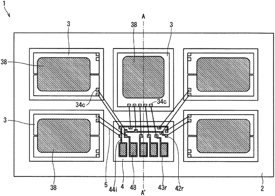
1. A semiconductor package comprising:
a conductor substrate;
a plurality of semiconductor elements having a switching function and bonded to a first main surface of the conductor substrate; and
a wiring element bonded to the first main surface of the conductor substrate, wherein
each of the plurality of semiconductor elements includes:
a first substrate,
a first main electrode arranged on a surface of the first substrate opposite to the conductor substrate,
a second main electrode arranged on a surface of the first substrate on a conductor substrate side and bonded to the conductor substrate, and
a control pad configured to control a current flowing between the first main electrode and the second main electrode,
the wiring element includes:
a second substrate,
a plurality of first relay pads arranged on a surface of the second substrate opposite to the conductor substrate and connected to each of the control pads of the plurality of semiconductor elements by wires,
a plurality of second relay pads arranged on the surface of the second substrate opposite to the conductor substrate, the number of the second relay pads being equal to or lower than the number of the plurality of first relay pads, and
a plurality of wiring portions arranged on the surface of the second substrate opposite to the conductor substrate and selectively connecting the plurality of first relay pads and the plurality of second relay pads, and
the semiconductor package further comprising:
a plurality of first conductor members bonded to the first main electrodes of the plurality of semiconductor elements;
a plurality of second conductor members bonded to the plurality of second relay pads of the wiring element; and
a sealing material covering the plurality of semiconductor elements, the wiring element, at least a part the plurality of first conductor members, at least a part of the plurality of second conductor members, and the first main surface of the conductor substrate, with an exposed surface being a surface of the plurality of first conductor members on the opposite side of the conductor substrate exposed, with an exposed surface being a surface of the plurality of second conductor members on the opposite side of the conductor substrate exposed, and with a second main surface of the conductor substrate on an opposite side of the first main surface exposed.
|