| CPC H01L 25/0657 (2013.01) [H01L 22/32 (2013.01); H01L 24/08 (2013.01); H01L 2224/08145 (2013.01); H01L 2225/06596 (2013.01)] | 19 Claims |

|
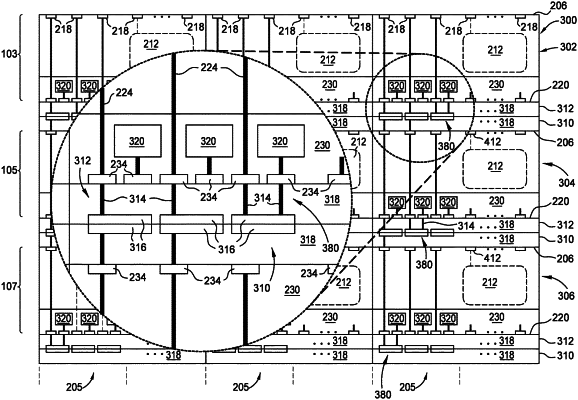
1. An integrated circuit (IC) device comprising:
a first wafer having a plurality of IC dies formed thereon separated by scribe lanes, the first wafer having a first front side bond pad disposed on an active side and coupled with a first back side bond pad disposed on a back side of the first wafer, and a second front side bond pad disposed on the active side and coupled to a second back side bond pad disposed on the back side of the first wafer;
a second wafer having a plurality of IC dies formed thereon separated by scribe lanes, the second wafer having a first front side bond pad disposed on an active side and coupled with a first backside bond pad disposed on a back side of the second wafer, and a second front side bond pad disposed on the active side and coupled to a second back side bond pad disposed on the back side of the second wafer;
a first test key formed in one of the scribe lanes of the first wafer;
a first hybrid bond interface layer coupling the first wafer to the second wafer, the first hybrid bond interface layer having a first U-turn connection that couples the first back side bond pad to the first test key;
a second test key disposed in one of the scribe lanes of the second wafer; and
a second hybrid bond interface layer formed on the second wafer, the second hybrid bond interface layer having a second U-turn connection that couples the second back side bond pad of the second wafer to the second test key;
wherein the second back side bond pad of the first wafer is aligned with and connected to the second front side bond pad of the second wafer through the first hybrid bond interface layer, and
wherein the second back side bond pad of the second wafer is connected to a back side test key bond pad of the second test key disposed in the second wafer through the second hybrid bond interface layer.
|