| CPC H01L 25/0657 (2013.01) [H01L 24/24 (2013.01); H01L 25/0652 (2013.01); H01L 25/105 (2013.01); H01L 25/18 (2013.01); H01L 24/08 (2013.01); H01L 2224/08145 (2013.01); H01L 2224/08235 (2013.01); H01L 2224/24227 (2013.01); H01L 2225/06517 (2013.01); H01L 2225/06544 (2013.01); H01L 2225/06548 (2013.01); H01L 2225/06555 (2013.01); H01L 2225/06568 (2013.01); H01L 2225/1035 (2013.01); H01L 2225/1058 (2013.01)] | 20 Claims |
|
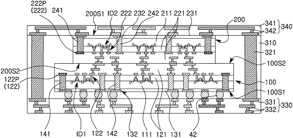
1. A semiconductor package, comprising:
a first semiconductor chip having a first front surface and a first rear surface, opposite to the first front surface, including:
a first circuit layer including a plurality of first individual devices and a first circuit wiring structure electrically connected to the plurality of first individual devices and providing the first front surface,
a first wiring layer including a first wiring structure and providing the first rear surface,
a first substrate layer disposed between the first circuit layer and the first wiring layer, and
a first through via for power penetrating through the first substrate layer and electrically connecting the first circuit wiring structure and the first wiring structure with each other; and
a second semiconductor chip disposed on the first semiconductor chip, having a second front surface and a second rear surface, opposite to the second front surface, including:
a second circuit layer including a plurality of second individual devices and a second circuit wiring structure electrically connected to the plurality of second individual devices and providing the second front surface,
a second wiring layer including a second wiring structure and providing the second rear surface,
a second substrate layer disposed between the second circuit layer and the second wiring layer, and
a second through via for power penetrating through the second substrate layer and electrically connecting the second circuit wiring structure and the second wiring structure with each other,
wherein the first and second semiconductor chips have different widths in a direction, parallel to the first and second front surfaces,
wherein the first semiconductor chip receives power through the first wiring structure and the first through via for power, and
wherein the second semiconductor chip receives power through the second wiring structure and the second through via for power.
|