| CPC H01L 25/0652 (2013.01) [H01L 21/486 (2013.01); H01L 21/561 (2013.01); H01L 21/78 (2013.01); H01L 23/3128 (2013.01); H01L 23/49827 (2013.01); H01L 24/16 (2013.01); H01L 2224/16225 (2013.01)] | 25 Claims |
|
1. A semiconductor package, comprising:
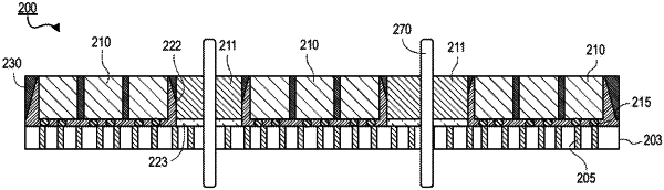
a plurality of dies on a substrate, the substrate having a first straight edge laterally opposite to a second straight edge, the substrate comprising silicon, the substrate having semiconductor structures, and the substrate having through substrate vias (TSVs);
an encapsulation layer over the substrate, wherein the encapsulation layer surrounds the plurality of dies; and
a plurality of dummy silicon regions on the substrate, wherein the plurality of dummy silicon regions have a top surface that is substantially coplanar to a top surface of the plurality of dies, and wherein the plurality of dummy silicon regions comprises a first dummy silicon die and a second dummy silicon die, the second dummy silicon die discontinuous with the first dummy silicon die, the first dummy silicon die proximate to the first straight edge of the substrate, and the second dummy silicon die proximate to the second straight edge of the substrate.
|