| CPC H01L 24/81 (2013.01) [H01L 24/16 (2013.01); H01L 24/17 (2013.01); H01L 25/18 (2013.01); H01L 25/50 (2013.01); H01L 2224/16145 (2013.01); H01L 2224/16227 (2013.01); H01L 2224/1703 (2013.01); H01L 2224/17181 (2013.01); H01L 2224/17505 (2013.01); H01L 2224/81005 (2013.01); H01L 2224/81192 (2013.01); H01L 2924/15153 (2013.01)] | 20 Claims |
|
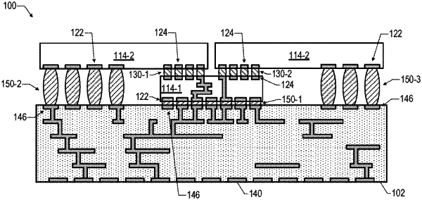
1. A microelectronic assembly, comprising:
a package substrate having an uppermost surface;
a first die entirely above the uppermost surface of the package substrate, the first die coupled to the package substrate, the first die having a first sidewall and a second sidewall, the second sidewall laterally opposite the first sidewall, the first die comprising through silicon vias, the through silicon vias coupled to the package substrate;
first interconnects entirely above the uppermost surface of the package substrate, the first interconnects laterally spaced apart from the first sidewall of the first die, the first interconnects coupled to the package substrate, and the first interconnects extending an entire vertical length of the first die;
second interconnects entirely above the uppermost surface of the package substrate, the second interconnects laterally spaced apart from the second sidewall of the first die, the second interconnects coupled to the package substrate, and the second interconnects extending the entire vertical length of the first die;
a second die vertically over the first interconnects and a first portion of the first die, the second die coupled to the first interconnects and to the first portion of the first die; and
a third die vertically over the second interconnects and a second portion of the first die, the third die coupled to the second interconnects and to the second portion of the first die, the third die laterally spaced apart from the second die.
|