| CPC H01L 24/48 (2013.01) [H01L 24/04 (2013.01); H01L 24/78 (2013.01); H01L 24/85 (2013.01); H01L 2224/04042 (2013.01); H01L 2224/4805 (2013.01); H01L 2224/4807 (2013.01); H01L 2224/4845 (2013.01); H01L 2224/48451 (2013.01); H01L 2224/48453 (2013.01); H01L 2224/48463 (2013.01); H01L 2224/48482 (2013.01); H01L 2224/7895 (2013.01); H01L 2224/8503 (2013.01); H01L 2924/381 (2013.01)] | 11 Claims |
|
1. A semiconductor device comprising:
an integrated circuit die having a plurality of bond pads; and
a plurality of bond wires, each of the plurality of bond wires being physically connected to a respective one of the plurality of bond pads by a ball bond,
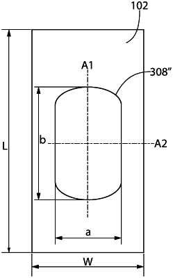
wherein a footprint of each ball bond in an area of contact between each ball bond and the respective bond pad has a shape that is non-circular and includes a first axis of symmetry,
wherein the footprint of each ball bond includes a ball bond width and a ball bond length, and
wherein each of the bond pads includes a bond pad width and a bond pad length, and wherein a ratio of the ball bond length to the ball bond width is equal to a ratio of the bond pad length to the bond pad width ±10%.
|