| CPC H01L 24/20 (2013.01) [H01L 23/3135 (2013.01); H01L 24/13 (2013.01); H01L 24/19 (2013.01); H01L 24/96 (2013.01); H01L 24/97 (2013.01); H01L 2224/13023 (2013.01); H01L 2224/2101 (2013.01)] | 12 Claims |
|
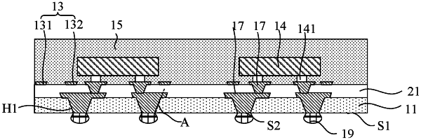
1. A chip package structure, comprising:
a chip, the chip including metal pins;
an organic polymer material layer, the organic polymer material layer being located on a side of the metal pins away from the chip, the organic polymer material layer including a first via hole, and the organic polymer material layer including a first surface away from the chip;
metal parts, at least a first portion of the metal parts being located in the first via hole, the metal parts and metal pins being electrically connected, the metal parts including a second surface away from the chip, and the second surface and the first surface being flush to each other;
an encapsulating layer, the encapsulating layer being located on a side of the metal parts away from the organic polymer material layer; and
an alignment part, wherein an orthographic projection of the chip on the organic polymer material layer borders on an orthographic projection of the alignment part on the organic polymer material layer.
|