| CPC H01L 24/13 (2013.01) [H01L 24/05 (2013.01); H01L 24/16 (2013.01); H01L 24/81 (2013.01); H01L 25/0657 (2013.01); H01L 25/50 (2013.01); H01L 2224/13017 (2013.01); H01L 2224/1355 (2013.01); H01L 2224/16059 (2013.01); H01L 2924/37001 (2013.01)] | 20 Claims |
|
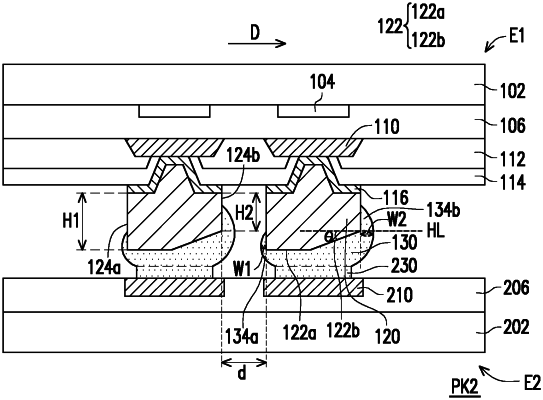
1. A semiconductor package, comprising:
a first conductive pillar, wherein the first conductive pillar has a first sidewall, a second sidewall opposite to the first sidewall, a first surface and a second surface physically connected to the first surface, the first surface and the second surface are disposed between the first sidewall and the second sidewall, and an included angle is formed between the first surface and the second surface, wherein a height of the first sidewall is greater than a height of the second sidewall;
a conductive pad; and
a solder region disposed between and in direct contact with the first conductive pillar and the conductive pad, wherein the solder region has a first convex sidewall on the second sidewall of the first conductive pillar.
|