| CPC H01L 24/08 (2013.01) [G06F 11/1008 (2013.01); G06F 11/1048 (2013.01); G11C 7/10 (2013.01); H01L 25/0657 (2013.01); H01L 25/18 (2013.01); H01L 25/50 (2013.01); H10B 41/20 (2023.02); H10B 41/40 (2023.02); H10B 41/50 (2023.02); H10B 43/20 (2023.02); H10B 43/40 (2023.02); H10B 43/50 (2023.02); H01L 2224/0603 (2013.01); H01L 2224/08145 (2013.01); H01L 2225/06524 (2013.01); H01L 2225/06541 (2013.01); H01L 2924/1431 (2013.01); H01L 2924/14511 (2013.01)] | 20 Claims |
|
1. A storage device comprising:
a nonvolatile memory (NVM) device comprising NVM cells; and
a memory controller configured to control the NVM device,
wherein the NVM device comprises
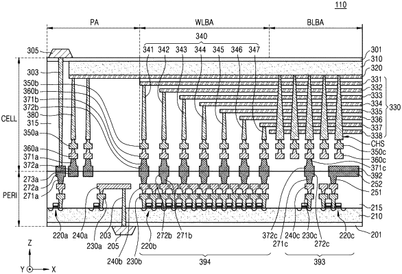
a first chip including a peripheral circuit region comprising a first control logic circuit configured to control operation modes of the NVM device, the peripheral circuit region being on a first surface of a first substrate of the first chip; and
a second chip including three-dimensional (3D) arrays of the NVM cells, the 3D arrays being on a first surface of a second substrate of the second chip, and the second chip being vertically stacked on the first chip so that the first surface of the first substrate is bonded with the first surface of the second substrate, and
wherein the memory controller comprises
a third chip including a control circuit region comprising circuits configured to set and change operation conditions of the NVM device, the control circuit region being on a first surface of a third substrate of the third chip, and a second control logic circuit associated with the operation conditions of the NVM device being on the first surface of the third substrate of the third chip.
|