| CPC H01L 24/06 (2013.01) [H01L 21/565 (2013.01); H01L 21/76885 (2013.01); H01L 23/3185 (2013.01); H01L 23/488 (2013.01); H01L 24/03 (2013.01); H01L 24/05 (2013.01); H01L 24/16 (2013.01); H01L 24/19 (2013.01); H01L 24/20 (2013.01); H01L 24/81 (2013.01); H01L 21/6835 (2013.01); H01L 24/11 (2013.01); H01L 24/32 (2013.01); H01L 24/73 (2013.01); H01L 24/83 (2013.01); H01L 24/92 (2013.01); H01L 25/105 (2013.01); H01L 2221/68359 (2013.01); H01L 2224/0345 (2013.01); H01L 2224/03462 (2013.01); H01L 2224/03464 (2013.01); H01L 2224/0401 (2013.01); H01L 2224/04105 (2013.01); H01L 2224/05015 (2013.01); H01L 2224/05024 (2013.01); H01L 2224/05082 (2013.01); H01L 2224/05124 (2013.01); H01L 2224/05139 (2013.01); H01L 2224/05144 (2013.01); H01L 2224/05147 (2013.01); H01L 2224/05155 (2013.01); H01L 2224/05164 (2013.01); H01L 2224/05166 (2013.01); H01L 2224/05181 (2013.01); H01L 2224/05555 (2013.01); H01L 2224/06131 (2013.01); H01L 2224/06179 (2013.01); H01L 2224/06515 (2013.01); H01L 2224/11334 (2013.01); H01L 2224/11849 (2013.01); H01L 2224/12105 (2013.01); H01L 2224/13111 (2013.01); H01L 2224/13116 (2013.01); H01L 2224/13139 (2013.01); H01L 2224/13147 (2013.01); H01L 2224/16145 (2013.01); H01L 2224/16227 (2013.01); H01L 2224/18 (2013.01); H01L 2224/19 (2013.01); H01L 2224/32225 (2013.01); H01L 2224/73267 (2013.01); H01L 2224/81805 (2013.01); H01L 2224/83005 (2013.01); H01L 2224/838 (2013.01); H01L 2224/83874 (2013.01); H01L 2224/92244 (2013.01); H01L 2225/1035 (2013.01); H01L 2225/1041 (2013.01); H01L 2225/1058 (2013.01); H01L 2924/014 (2013.01); H01L 2924/01322 (2013.01); H01L 2924/04941 (2013.01); H01L 2924/04953 (2013.01); H01L 2924/15311 (2013.01); H01L 2924/2064 (2013.01); H01L 2924/3512 (2013.01); H01L 2924/35121 (2013.01)] | 20 Claims |
|
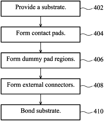
1. A method of forming a semiconductor device, the method comprising:
forming contact pads over a first substrate; and
forming dummy pad features over the first substrate, each of the dummy pad features being adjacent to a corresponding one of the contact pads, each of the dummy pad features being electrically disconnected from the corresponding one of the contact pads, wherein no other conductive material is interposed directly between each of the dummy pad features and the corresponding one of the contact pads.
|