| CPC H01L 24/05 (2013.01) [H01L 21/481 (2013.01); H01L 21/486 (2013.01); H01L 21/56 (2013.01); H01L 21/561 (2013.01); H01L 23/3114 (2013.01); H01L 23/3135 (2013.01); H01L 23/481 (2013.01); H01L 23/49811 (2013.01); H01L 23/49833 (2013.01); H01L 23/49838 (2013.01); H01L 23/49861 (2013.01); H01L 23/49866 (2013.01); H01L 23/5389 (2013.01); H01L 24/07 (2013.01); H01L 24/13 (2013.01); H01L 24/19 (2013.01); H01L 24/96 (2013.01); H01L 21/568 (2013.01); H01L 23/49827 (2013.01); H01L 2224/0239 (2013.01); H01L 2224/02372 (2013.01); H01L 2224/0401 (2013.01); H01L 2224/05083 (2013.01); H01L 2224/05144 (2013.01); H01L 2224/05147 (2013.01); H01L 2224/05155 (2013.01); H01L 2224/05166 (2013.01); H01L 2224/05171 (2013.01); H01L 2224/05184 (2013.01); H01L 2224/12105 (2013.01); H01L 2224/13111 (2013.01); H01L 2224/13139 (2013.01); H01L 2224/13147 (2013.01); H01L 2224/2919 (2013.01); H01L 2224/2929 (2013.01); H01L 2224/29386 (2013.01); H01L 2224/83191 (2013.01); H01L 2224/94 (2013.01); H01L 2924/01029 (2013.01); H01L 2924/18162 (2013.01)] | 20 Claims |
|
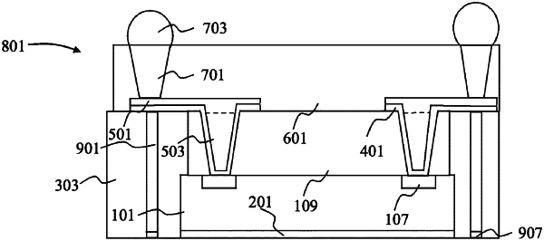
1. A method of manufacturing a semiconductor device, the method comprising:
forming a first surface, wherein the first surface comprises a protective material and an encapsulating material, wherein the protective material extends a first distance from the first surface to a second surface opposite the first surface and wherein the encapsulating material extends a second distance from the first surface to a third surface opposite the first surface, the second distance being greater than the first distance, wherein a semiconductor die is in physical contact with the second surface of the protective material and wherein the semiconductor die extends a third distance from the second surface to a fourth surface facing away from the second surface, wherein the second distance is at least as large as a sum of the first distance and the third distance, wherein the protective material has a first width and the semiconductor die has a second width greater than the first width; and
forming a conductive material extending over both the protective material and the encapsulating material, the conductive material also extending through the protective material to be in electrical contact with the semiconductor die, wherein the conductive material comprises a seed layer.
|