| CPC H01L 24/05 (2013.01) [H01L 23/5226 (2013.01); H01L 24/03 (2013.01); H01L 23/53228 (2013.01); H01L 23/53257 (2013.01); H01L 2224/024 (2013.01); H01L 2224/0235 (2013.01); H01L 2224/0239 (2013.01); H01L 2224/02313 (2013.01); H01L 2224/02372 (2013.01); H01L 2224/02375 (2013.01); H01L 2224/02381 (2013.01); H01L 2224/0391 (2013.01); H01L 2224/05546 (2013.01); H01L 2224/05624 (2013.01); H01L 2924/1438 (2013.01); H01L 2924/14511 (2013.01)] | 16 Claims |
|
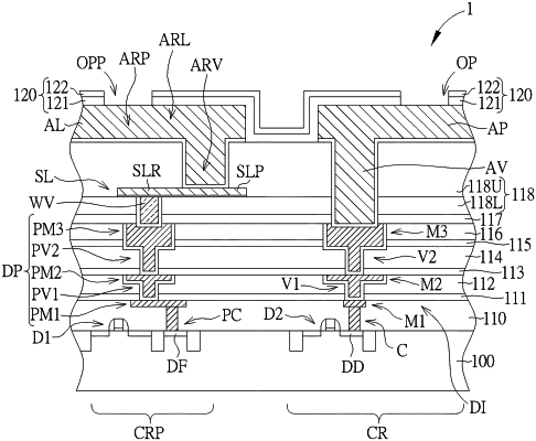
1. An integrated circuit structure, comprising:
a substrate comprising thereon a logic core circuit region and an embedded memory area;
a copper interconnect structure disposed on the substrate, wherein the copper interconnect structure comprises an uppermost copper layer covered by a dielectric layer;
an aluminum pad layer disposed on the dielectric layer, wherein the aluminum pad layer comprises a first pad pattern within the logic core circuit region and a second pad pattern within the embedded memory area;
a passivation layer covering the first pad pattern within the logic core circuit region and the second pad pattern within the embedded memory area; and
an aluminum shield layer comprising concentric aluminum routing patterns disposed directly on the embedded memory area and between the uppermost copper layer and the aluminum pad layer, wherein the aluminum shield layer has a thickness that is thinner than that of the aluminum pad layer, wherein the first pad pattern and the second pad pattern respectively contact the uppermost copper layer and the aluminum shield layer at different horizontal levels.
|
|
11. A method for forming an integrated circuit structure, comprising:
providing a substrate comprising thereon a logic core circuit region and an embedded memory area;
forming a copper interconnect structure on the substrate, wherein the copper interconnect structure comprises an uppermost copper layer covered by a dielectric layer;
forming an aluminum shield layer comprising concentric aluminum routing patterns on the uppermost copper layer in the embedded memory area; and
forming an aluminum pad layer on the dielectric layer, wherein the aluminum shield layer has a thickness that is thinner than that of the aluminum pad layer, wherein the aluminum pad layer comprises a first pad pattern within the logic core circuit region and a second pad pattern within the embedded memory area; and
forming a passivation layer covering the first pad pattern within the logic core circuit region and the second pad pattern within the embedded memory area.
|