| CPC H01L 23/562 (2013.01) [H01L 25/0652 (2013.01); H01L 25/18 (2013.01); H01L 23/32 (2013.01); H01L 23/5386 (2013.01)] | 23 Claims |

|
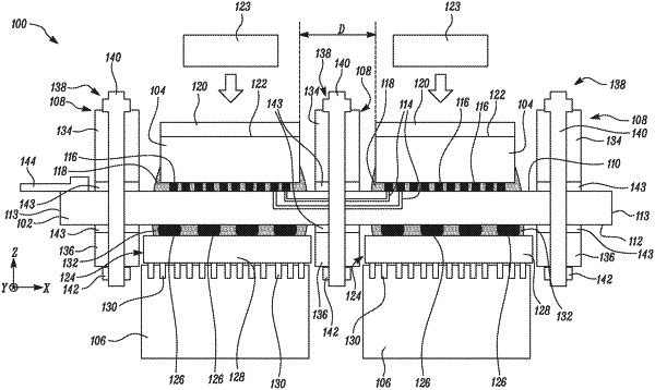
1. An electronic assembly comprising:
a substrate comprising a first surface and a second surface opposite to the first surface, the substrate further comprising a plurality of substrate interconnects;
a plurality of semiconductor dies mounted on the first surface of the substrate, wherein the plurality of semiconductor dies are electrically connected to each other via the plurality of substrate interconnects;
a plurality of power supply modules mounted on the second surface of the substrate, wherein each power supply module is disposed opposite to a respective semiconductor die; and
a plurality of stiffening members coupled to the substrate, wherein the plurality of stiffening members are configured to control warpage of the substrate, and wherein individual stiffening members comprise:
a first stiffening portion disposed on the first surface of the substrate; and
a second stiffening portion disposed on the second surface of the substrate.
|