| CPC H01L 23/552 (2013.01) [H01L 21/56 (2013.01); H01L 23/3107 (2013.01); H01L 23/36 (2013.01); H01L 23/49503 (2013.01); H01L 24/32 (2013.01); H01L 2224/32245 (2013.01)] | 20 Claims |
|
1. A device comprising:
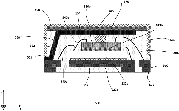
a package substrate having a die attach pad (DAP) and package pads;
a die disposed on the DAP, the die is electrically coupled to the package pads;
a primary electromagnetic interference (EMI) shield structure, the primary EMI shield structure comprises
a primary EMI planar member covering the die,
a first primary EMI leg member contiguous to a first side of the primary EMI planar member and extending downwards to the package substrate, the primary EMI shield structure forms a cavity over the die in which a cavity height of the cavity is defined by the first primary EMI leg member, wherein adjacent opposing sides of the first side of the primary EMI planar member do not include leg members extending downwards to the package substrate, leaving the die exposed on the adjacent opposing sides of the primary EMI planar member, and
wherein the primary EMI shield structure is electrically coupled to ground; and
an encapsulant, the encapsulant covers the first primary EMI leg member and the package substrate.
|