| CPC H01L 23/544 (2013.01) [H01L 21/0274 (2013.01); H01L 21/3083 (2013.01); H01L 2223/54426 (2013.01)] | 20 Claims |
|
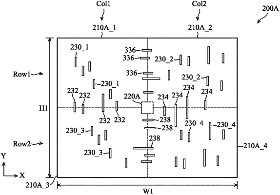
1. A semiconductor structure, comprising:
a plurality of product regions over a semiconductor substrate;
an alignment region over the semiconductor substrate and surrounded by the product regions;
a plurality of first features formed in a material layer over the semiconductor substrate; and
a plurality of second features formed in the material layer over the semiconductor substrate,
wherein the alignment regions is surrounded by and in physical contact with four of the product regions of a group, and each of the product regions in the group is adjacent to and in physical contact with two other product regions,
wherein each of the first features extends across two adjacent product regions, and each of the second features is disposed within one of the product regions, and wherein the first features are spaced apart from the second features,
wherein the alignment region is free of the first and second features.
|