| CPC H01L 23/544 (2013.01) [H01L 21/78 (2013.01); H01L 23/528 (2013.01); H01L 23/5223 (2013.01); H01L 28/40 (2013.01); H01L 21/02063 (2013.01); H01L 21/31144 (2013.01); H01L 28/60 (2013.01); H01L 28/90 (2013.01); H01L 28/91 (2013.01); H01L 29/00 (2013.01); H01L 2223/5442 (2013.01); H01L 2223/5446 (2013.01); H01L 2223/54426 (2013.01); H01L 2223/54453 (2013.01); H10B 12/37 (2023.02)] | 20 Claims |

|
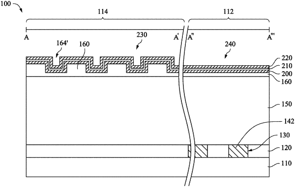
1. A method of fabricating a semiconductor structure, comprising:
forming an alignment mark layer over a substrate;
patterning the alignment mark layer to define a first alignment mark feature and a second alignment mark feature from the alignment mark layer; and
forming a bottom conductive layer over the first alignment mark feature and the second alignment mark feature and between the first alignment mark feature and the second alignment mark feature.
|