| CPC H01L 23/5389 (2013.01) [H01L 21/4853 (2013.01); H01L 21/4857 (2013.01); H01L 21/565 (2013.01); H01L 21/568 (2013.01); H01L 21/6835 (2013.01); H01L 23/3128 (2013.01); H01L 23/3135 (2013.01); H01L 23/5383 (2013.01); H01L 23/5386 (2013.01); H01L 24/16 (2013.01); H01L 24/19 (2013.01); H01L 24/20 (2013.01); H01L 25/105 (2013.01); H01L 25/18 (2013.01); H01L 2221/68372 (2013.01); H01L 2224/16227 (2013.01); H01L 2224/214 (2013.01); H01L 2225/1035 (2013.01); H01L 2225/1058 (2013.01); H01L 2924/1431 (2013.01); H01L 2924/1434 (2013.01); H01L 2924/18161 (2013.01)] | 19 Claims |
|
1. A semiconductor package comprising:
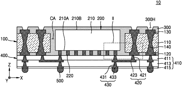
a frame structure comprising a core portion and a plurality of lower pads under the core portion, wherein a cavity penetrates the core portion;
a semiconductor chip arranged in the cavity, wherein the semiconductor chip comprises an active surface on which a plurality of bump pads are arranged and a non-active surface opposite the active surface, wherein the bump pads protrude from the active surface of the semiconductor chip and have a polygonal column shape or a cylindrical shape;
a redistribution structure under the frame structure and the semiconductor chip, wherein the redistribution structure is connected to the lower pads and the bump pads; and
a molding member that is on the frame structure and the semiconductor chip, and that is in the cavity,
wherein the molding member surrounds a lower surface of the frame structure, the active surface of the semiconductor chip, the lower pads, and the bump pads, wherein the molding member contacts a side surface of the bump pads, wherein the molding member covers an upper surface of the core portion, a lower surface of the core portion, and a side surface of the core portion, and wherein the molding member fills a space between the lower pads and a space between the bump pads, and wherein the molding member contacts an upper surface of the redistribution structure.
|