| CPC H01L 23/535 (2013.01) [H01L 21/76805 (2013.01); H01L 21/76843 (2013.01); H01L 21/76895 (2013.01); H10B 12/0335 (2023.02); H10B 12/053 (2023.02); H10B 12/09 (2023.02); H10B 12/315 (2023.02); H10B 12/34 (2023.02); H10B 12/482 (2023.02); H10B 12/485 (2023.02); H10B 12/50 (2023.02)] | 20 Claims |
|
1. A method of manufacturing a semiconductor memory device, the method comprising:
preparing a substrate including a cell area and a peripheral area;
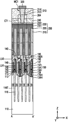
forming a plurality of lower electrodes on the cell area of the substrate;
forming a capacitor dielectric layer covering the plurality of lower electrodes;
forming an upper electrode, wherein the forming the upper electrode includes forming a first upper electrode layer covering the capacitor dielectric layer and including a semiconductor material, and forming a second upper electrode layer covering the first upper electrode layer and including a metallic material;
forming a filling insulation layer on the second upper electrode layer, the filling insulation layer having a first wiring contact hole;
forming a first wiring contact plug filling the first wiring contact hole, the first wiring contact plug electrically connecting to the upper electrode, and
forming a plurality of wiring lines on the filling insulation layer, at least one of the plurality of wiring lines electrically connecting to the first wiring contact plug.
|