| CPC H01L 23/5329 (2013.01) [H01L 23/293 (2013.01); H01L 23/5226 (2013.01); H01L 21/4853 (2013.01); H01L 23/50 (2013.01); H01L 23/5381 (2013.01); H01L 23/5385 (2013.01); H01L 24/19 (2013.01); H01L 24/25 (2013.01)] | 20 Claims |

|
1. A die interconnect substrate, comprising:
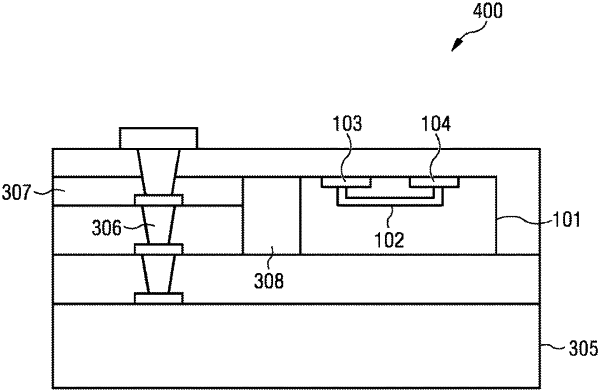
a bridge die having a top side above a bottom side, and a first sidewall and a second sidewall between the top side and the bottom side, the first sidewall laterally opposite the second sidewall, the bridge die having a bridge die pad;
a substrate interconnect laterally spaced apart from the first sidewall of the bridge die;
an insulating filler structure laterally between the substrate interconnect and the bridge die, the insulating filler structure in contact with the first sidewall of the bridge die;
an insulating layer on and in direct contact with the substrate interconnect, on the insulating filler structure, and on the bridge die;
a vertical wiring layer in a first opening in the insulating layer, the vertical wiring layer on the substrate interconnect;
a first lateral wiring layer on the vertical wiring layer and on the insulating layer;
a first contact interface structure on the first lateral wiring layer;
a via portion in a second opening in the insulating layer, the via portion on the bridge die pad;
a second lateral wiring layer on the via portion and on the insulating layer; and
a second contact interface structure on the second lateral wiring layer.
|