| CPC H01L 23/5329 (2013.01) [H01L 21/0214 (2013.01); H01L 21/0228 (2013.01); H01L 21/02126 (2013.01); H01L 21/02211 (2013.01); H01L 21/02219 (2013.01); H01L 21/02271 (2013.01); H01L 21/76224 (2013.01); H01L 21/76834 (2013.01); H01L 21/76843 (2013.01); H01L 21/76877 (2013.01); H01L 23/481 (2013.01); H01L 23/5283 (2013.01); H01L 23/53223 (2013.01); H01L 23/53238 (2013.01); H01L 27/1463 (2013.01); H01L 27/14614 (2013.01); H01L 27/14634 (2013.01); H01L 27/14636 (2013.01); H01L 27/14643 (2013.01); H01L 27/14687 (2013.01); H01L 21/76831 (2013.01); H01L 23/485 (2013.01)] | 20 Claims |
|
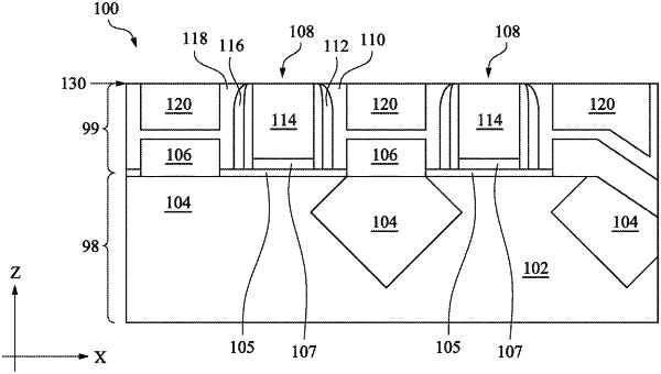
1. A structure, comprising:
a substrate;
a dielectric layer that contains nitrogen or carbon, wherein a concentration of nitrogen or a concentration of carbon varies within the dielectric layer based on a distance away from a bottom surface of the dielectric layer;
a first photo-sensitive element and a second photo-sensitive element disposed over the substrate;
a first color filter and a second color filter disposed over the first photo-sensitive element and over the second photo-sensitive element, respectively; and
a first micro lens and a second micro lens disposed over the first color filter and the second color filter, respectively.
|