| CPC H01L 23/5283 (2013.01) [H01L 28/60 (2013.01); H01L 28/75 (2013.01); H01L 28/90 (2013.01)] | 16 Claims |
|
1. A semiconductor device comprising:
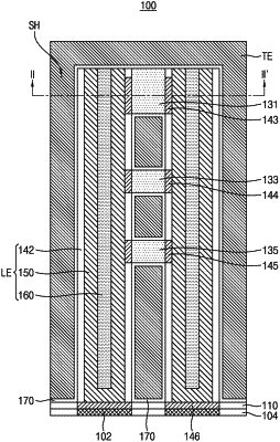
a landing pad on a substrate;
a lower electrode on the landing pad, the lower electrode including an outer protective layer, a conductive layer between opposing sidewalls of the outer protective layer, and an inner protective layer between opposing sidewalls of the conductive layer;
a first supporter pattern on a side surface of the lower electrode, the first supporter pattern including a supporter hole;
a first metal layer between the conductive layer and the first supporter pattern;
a dielectric layer on a surface of each of the lower electrode and the first supporter pattern; and
an upper electrode on the dielectric layer,
wherein an upper end of the outer protective layer is at a higher level than an upper surface of the conductive layer,
wherein the outer protective layer includes titanium oxide, the conductive layer includes titanium nitride, and the inner protective layer includes titanium silicon nitride,
wherein, in a horizontal cross-sectional view, the outer protective layer has an arc shape that extends between the dielectric layer and the conductive layer, and
wherein the first metal layer overlaps the outer protective layer in a vertical direction.
|