US 11,901,289 B2
Semiconductor device structure with resistive element
Wan-Te Chen, New Taipei (TW); Chung-Hui Chen, Hsinchu (TW); Wei-Chih Chen, Hsinchu (TW); Chii-Ping Chen, Hsinchu (TW); Wen-Sheh Huang, Hsinchu (TW); Bi-Ling Lin, Hsinchu (TW); and Sheng-Feng Liu, Taipei (TW)
Assigned to TAIWAN SEMICONDUCTOR MANUFACTURING COMPANY, LTD., Hsinchu (TW)
Filed by TAIWAN SEMICONDUCTOR MANUFACTURING COMPANY, LTD., Hsinchu (TW)
Filed on Jun. 23, 2022, as Appl. No. 17/848,146.
Application 17/848,146 is a continuation of application No. 16/422,101, filed on May 24, 2019, granted, now 11,404,369.
Application 16/422,101 is a continuation of application No. 15/599,687, filed on May 19, 2017, granted, now 10,304,772, issued on May 28, 2019.
Prior Publication US 2022/0319987 A1, Oct. 6, 2022
This patent is subject to a terminal disclaimer.
Int. Cl. H01L 23/522 (2006.01); H01L 27/06 (2006.01); H01L 23/367 (2006.01); H01L 29/423 (2006.01); H01L 29/78 (2006.01)
CPC H01L 23/5228 (2013.01) [H01L 23/3677 (2013.01); H01L 27/0629 (2013.01); H01L 29/42376 (2013.01); H01L 29/78 (2013.01)] 20 Claims
OG exemplary drawing
 
1. A semiconductor device structure, comprising:
a substrate;
a resistive element over the substrate; and
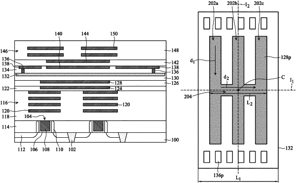
a thermal conductive element over the substrate, wherein a direct projection of the thermal conductive element on a main surface of the resistive element extends across a portion of a first imaginary line and a portion of a second imaginary line of the main surface, the first imaginary line is perpendicular to the second imaginary line, and the first imaginary line and the second imaginary line intersect at a center of the main surface.