| CPC H01L 23/5226 (2013.01) [H01L 21/76816 (2013.01); H10B 69/00 (2023.02)] | 24 Claims |
|
1. A microelectronic device, comprising:
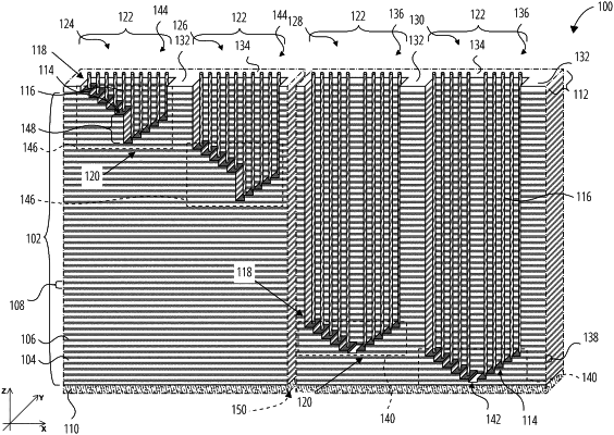
a stack structure comprising a vertically alternating sequence of insulative structures and conductive structures arranged in tiers, each of the tiers comprising at least one of the conductive structures and at least one of the insulative structures;
stadiums within the stack structure, at least one of the stadiums comprising two staircases having steps provided by a group of the conductive structures, each of the conductive structures of the group individually providing a continuous conductive region across the two staircases of the at least one of the stadiums; and
step contacts extending to the steps of the two staircases of the at least one of the stadiums, each conductive structure of the group of conductive structures having more than one of the step contacts in contact therewith at at least one of the steps of the two staircases.
|
|
19. A microelectronic device, comprising:
a stack structure comprising insulative structures vertically interleaved with conductive structures and arranged in tiers;
a series of stadiums in the stack structure, at least one of the stadiums having steps at least partially defined by the conductive structures of a first group of the tiers, and at least one other of the stadiums having additional steps at least partially defined by the conductive structures of a second group of the tiers, the first group of the tiers being at elevations lower than elevations of the second group of the tiers; and
conductive contacts within horizontal areas of stadiums of the series of stadiums, the conductive contacts comprising:
pairs of the conductive contacts, each of the pairs of the conductive contacts extending to a different one of the conductive structures of the first group of the tiers than each other of the pairs of the conductive contacts; and
ones of the conductive contacts each extending to a different one of the conductive structures of the second group of the tiers than each other of the ones of the conductive contacts.
|
|
20. A method of forming a microelectronic device, the method comprising:
forming a tiered stack on a base structure, the tiered stack comprising a vertically alternating sequence of insulative structures and other structures;
forming stadiums in the tiered stack, each of the stadiums including one or more staircases at least partially defined by horizontal ends of some of the other structures, forming the stadiums in the tiered stack comprising:
defining, in upper elevations of the tiered stack, staircase profiles for the stadiums; and
extending the staircase profiles of at least some of the stadiums to lower elevations within the tiered stack than elevations of the staircase profiles of at least some others of the stadiums;
forming at least one dielectric material within trenches vertically overlying the stadiums;
forming contact openings through the at least one dielectric material, at least one pair of the contact openings vertically extending to a common one of the other structures; and
forming a conductive contact structure in each of the contact openings.
|
|
24. An electronic system, comprising:
a three-dimensional memory device comprising:
a stack structure comprising conductive structures vertically alternating with insulative structures and arranged in tiers;
a series of staircased stadiums defined in a block of the stack structure; and
pairs of step contacts extending, through dielectric material overlying at least one of the stadiums, to mutual ones of the conductive structures defining at least one step of the at least one stadium, each of the mutual ones of the conductive structures individually defining a continuous conductive region across the series of staircased stadiums;
at least one processor in operable communication with the three-dimensional memory device; and
at least one peripheral device in operable communication with the at least one processor.
|