| CPC H01L 23/49822 (2013.01) [H01L 21/486 (2013.01); H01L 21/4857 (2013.01); H01L 21/56 (2013.01); H01L 21/561 (2013.01); H01L 21/563 (2013.01); H01L 21/565 (2013.01); H01L 21/568 (2013.01); H01L 21/6835 (2013.01); H01L 23/3185 (2013.01); H01L 23/49816 (2013.01); H01L 23/49833 (2013.01); H01L 23/49838 (2013.01); H01L 24/16 (2013.01); H01L 24/32 (2013.01); H01L 24/73 (2013.01); H01L 24/81 (2013.01); H01L 25/165 (2013.01); H01L 25/16 (2013.01); H01L 2221/68345 (2013.01); H01L 2224/16227 (2013.01); H01L 2224/16238 (2013.01); H01L 2224/32225 (2013.01); H01L 2224/73204 (2013.01); H01L 2224/81815 (2013.01); H01L 2924/15174 (2013.01)] | 20 Claims |
|
1. A semiconductor package, comprising:
a semiconductor die;
an encapsulant laterally encapsulating the semiconductor die; and
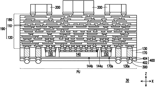
a redistribution structure disposed on the encapsulant along a stacking direction, overlapping with the semiconductor die and electrically connected with the semiconductor die, wherein the redistribution structure comprises a first conductive via, a first conductive wire, a second conductive via, a first dielectric layer and a second dielectric layer, the first conductive via, the first conductive wire and the second conductive via are arranged along the stacking direction, the first conductive via has a first via surface contacting the first conductive wire, the second conductive via has a second via surface contacting the first conductive wire, an area of a first cross section of the first conductive via is greater than an area of the first via surface of the first conductive via, an area of a second cross section of the second conductive via is greater than an area of the second via surface of the second conductive via, the first via surface of the first conductive via and the first conductive wire are wrapped by the first dielectric layer, the second via surface of the second conductive via is substantially coplanar with a bottom surface of the second dielectric layer, and the second conductive via is farther away the semiconductor die than the first conductive via.
|