| CPC H01L 23/49822 (2013.01) [H01L 21/486 (2013.01); H01L 21/4857 (2013.01); H01L 21/56 (2013.01); H01L 21/561 (2013.01); H01L 21/563 (2013.01); H01L 21/565 (2013.01); H01L 21/568 (2013.01); H01L 21/6835 (2013.01); H01L 23/3185 (2013.01); H01L 23/49816 (2013.01); H01L 23/49833 (2013.01); H01L 23/49838 (2013.01); H01L 24/16 (2013.01); H01L 24/32 (2013.01); H01L 24/73 (2013.01); H01L 24/81 (2013.01); H01L 25/165 (2013.01); H01L 25/16 (2013.01); H01L 2221/68345 (2013.01); H01L 2224/16227 (2013.01); H01L 2224/16238 (2013.01); H01L 2224/32225 (2013.01); H01L 2224/73204 (2013.01); H01L 2224/81815 (2013.01); H01L 2924/15174 (2013.01)] | 20 Claims |
|
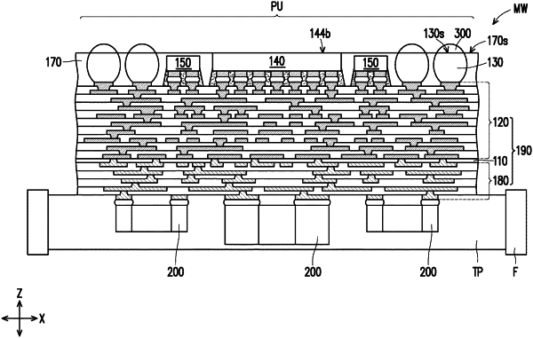
1. A semiconductor package, comprising:
a semiconductor die;
an encapsulant laterally encapsulating the semiconductor die; and
a redistribution structure disposed on the encapsulant along a first direction and electrically connected with the semiconductor die, wherein the redistribution structure comprises a first conductive via, a first conductive wire and a second conductive via arranged along the first direction, the first conductive via has a first surface contacting the first conductive wire and a second surface opposite to the first surface along the first direction, the second conductive via has a third surface contacting the first conductive wire and a fourth surface opposite to the third surface along the first direction, a lateral dimension of the second surface along a second direction is greater than a lateral dimension of the first surface along the second direction, and a lateral dimension of the fourth surface along the second direction is greater than a lateral dimension of the third surface along the second direction, and the second direction is perpendicular to the first direction, and wherein the redistribution structure further comprises a first dielectric layer and a second dielectric layer, the first dielectric layer surrounds the first conductive via and the first conductive wire, the second dielectric layer surrounds the second conductive via, and the first conductive via is closer to the semiconductor die than the second conductive via.
|