| CPC H01L 23/49816 (2013.01) [H01L 23/13 (2013.01); H01L 23/5386 (2013.01); H01L 25/0657 (2013.01); H01L 25/105 (2013.01); H01L 25/50 (2013.01)] | 20 Claims |
|
1. A packaged device comprising:
a first package material, the first package material having a first widest lateral width;
one or more integrated circuit (IC) dies disposed within the first package material;
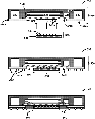
a first substrate coupled to the one or more IC dies and disposed in or on the first package material, wherein an opposing sidewalls of the first substrate define at least in part a recess structure extending from a first side of the first substrate and through the first substrate, the recess structure to receive a unit including another IC die, and the first substrate having a second widest lateral width, the second widest lateral width the same as the first widest lateral width;
an active or passive component on the first substrate and laterally spaced apart from the one or more IC dies, the active or passive component included in the first package material;
a first hardware interface to couple the packaged device to a second device, the first hardware interface including first contacts disposed on the first side of the first substrate;
a second hardware interface to couple one of the one or more IC dies to the other IC die, the second hardware interface including second contacts disposed in the recess structure;
a second substrate extending across the recess structure, wherein the second contacts are disposed on a side of the second substrate, wherein the second substrate is laterally surrounded by the first package material, and wherein the second substrate has a lateral width greater than a lateral width of the other IC die; and
a second package material on a bottom of the first substrate, on a bottom of the second substrate, and on a bottom of the other IC die, the second package material having a third widest lateral width the same as the second widest lateral width, the second package material laterally adjacent to the first contacts disposed on the first side of the first substrate, and the second package material laterally surrounding the other IC die.
|