| CPC H01L 23/49811 (2013.01) [H01L 21/486 (2013.01); H01L 21/4853 (2013.01); H01L 21/565 (2013.01); H01L 23/3171 (2013.01); H01L 23/49833 (2013.01); H01L 23/49844 (2013.01); H01R 12/585 (2013.01); H01L 23/49861 (2013.01)] | 18 Claims |
|
1. A method of forming a semiconductor device, the method comprising:
providing a substrate that comprises a metal region;
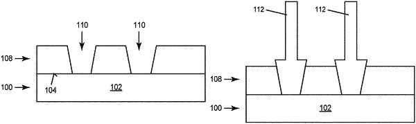
forming an encapsulant body of electrically insulating material on an upper surface of the metal region;
forming an opening in the encapsulant body; and
inserting a press-fit connector into the opening;
wherein after inserting the press-fit connector into the opening, the press-fit connector is securely retained to the substrate and an interfacing end of the press-fit connector is electrically accessible,
wherein the encapsulant body is formed by a molding process whereby liquified mold material is formed on the substrate and subsequently hardened, wherein forming the opening comprises arranging a fixed pin over the substrate prior to the molding process, and wherein the fixed pin prevents the liquified mold material from forming at a location corresponding to the opening.
|