| CPC H01L 23/49575 (2013.01) [H01L 23/06 (2013.01); H01L 23/5384 (2013.01); H01P 3/00 (2013.01)] | 20 Claims |
|
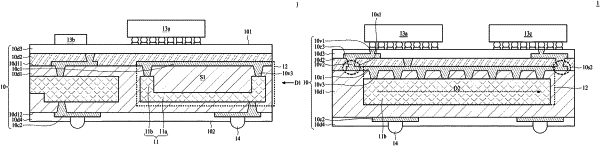
1. A semiconductor device package, comprising:
a conductive lid defining a waveguide having a cavity;
a dielectric layer encapsulating the conductive lid and partially disposed within the cavity,
a first conductive via partially penetrating the dielectric layer and connecting a bottom surface of the conductive lid,
wherein the waveguide is configured to transmit a signal from a first electronic component to a second electronic component through the cavity.
|