| CPC H01L 23/49568 (2013.01) [H01L 23/3178 (2013.01); H01L 23/367 (2013.01); H01L 23/3735 (2013.01); H01L 23/4334 (2013.01); H01L 23/49805 (2013.01); H01L 23/49827 (2013.01); H01L 2224/02371 (2013.01)] | 20 Claims |
|
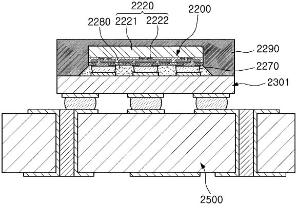
1. A semiconductor package, comprising:
a semiconductor chip having an active surface, on which a connection pad is disposed, and an inactive surface opposite to the active surface;
a heat-dissipating member disposed on the inactive surface of the semiconductor chip and comprising graphite;
an encapsulant sealing at least a portion of each of the semiconductor chip and the heat-dissipating member;
a capping metal layer disposed directly between the heat-dissipating member and the encapsulant; and
a connection structure disposed on the active surface of the semiconductor chip and comprising a redistribution layer electrically connected to the connection pad,
wherein the heat-dissipating member includes holes passing through at least a portion of the heat-dissipating member, and the holes overlap the inactive surface of the semiconductor chip.
|