| CPC H01L 23/481 (2013.01) [H01L 21/30608 (2013.01); H01L 21/76871 (2013.01)] | 20 Claims |
|
1. A method for forming a semiconductor device structure, comprising:
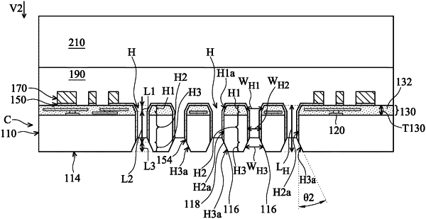
providing a chip structure comprising a substrate and a wiring structure over a first surface of the substrate, wherein the chip structure has a hole penetrating through the wiring structure and extending into the substrate;
removing a first portion of the wiring structure adjacent to the hole to widen a second portion of the hole in the wiring structure, wherein the second portion has a first width increasing in a first direction away from the substrate;
forming a first seed layer over the wiring structure and in the hole;
thinning the substrate from a second surface of the substrate until the first seed layer in the hole is exposed, wherein the second surface is opposite to the first surface, and the hole penetrates through the substrate after thinning the substrate; and
forming a second seed layer over the second surface of the substrate and the first seed layer in the hole, wherein the second seed layer is in direct contact with the first seed layer.
|