| CPC H01L 23/3185 (2013.01) [H01L 21/78 (2013.01); H01L 23/49822 (2013.01); H01L 23/5226 (2013.01); H01L 24/73 (2013.01); H01L 24/94 (2013.01); H01L 2224/73204 (2013.01)] | 20 Claims |
|
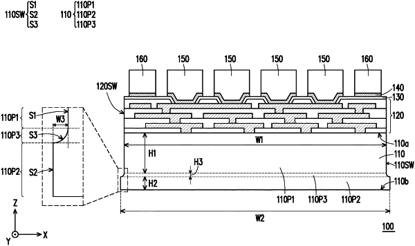
1. A semiconductor device, comprising:
a substrate having a first side, a second side and a sidewall connecting the first side and the second side, wherein the sidewall comprising a first planar sidewall of a first portion of the substrate, a second planar sidewall of a second portion of the substrate and a curved sidewall of a third portion of the substrate, wherein the first planar sidewall is connected to the second planar sidewall through the curved sidewall;
an interconnect structure, located on the first side of the substrate, wherein a sidewall of the interconnect structure is offset from the second planar sidewall; and
conductive vias, located on the interconnect structure, wherein the interconnect structure is located between the conductive vias and the substrate.
|