| CPC H01L 23/15 (2013.01) [H01L 21/486 (2013.01); H01L 23/3128 (2013.01); H01L 23/5381 (2013.01); H01L 23/5384 (2013.01); H01L 25/0655 (2013.01)] | 20 Claims |

|
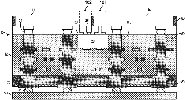
1. A semiconductor package, comprising:
a package substrate;
a glass core;
an insulator material at least partially encasing the glass core, wherein, along a direction perpendicular to a first surface of the glass core, a portion of the insulator material is between the glass core and the package substrate, and wherein a first surface of the package substrate is closer to the first surface of the glass core than a second surface of the package substrate;
a conductive via extending between the first surface of the glass core and a second surface of the glass core substantially in the direction perpendicular to the first surface of the glass core;
a bridge die in a recess in the package substrate and electrically coupled with the conductive via; and
an electronic component coupled to an end of the conductive via at the second surface of the package substrate.
|