| CPC H01L 22/22 (2013.01) [G01T 1/24 (2013.01); H01L 27/14659 (2013.01); H01L 27/14661 (2013.01); H01L 27/14689 (2013.01); H01L 27/14696 (2013.01); H01L 27/14698 (2013.01)] | 6 Claims |
|
1. A method comprising:
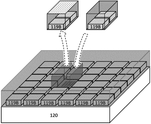
attaching a wafer to a substrate, wherein the substrate comprises discrete electrodes, wherein the wafer comprises a radiation absorption layer and a plurality of electrical contacts, wherein each of the electrical contacts is connected to at least one of the discrete electrodes;
identifying a defective area of the wafer;
replacing a portion of the wafer with at least one chip configured to absorb radiation, wherein the portion comprises the defective area.
|