| CPC H01L 21/823475 (2013.01) [H01L 21/76829 (2013.01); H01L 21/76897 (2013.01); H01L 21/823431 (2013.01); H01L 21/823481 (2013.01); H01L 23/5226 (2013.01); H01L 27/0886 (2013.01); H01L 29/0649 (2013.01); H01L 29/66795 (2013.01); H01L 29/785 (2013.01)] | 20 Claims |
|
1. A semiconductor device structure, comprising:
a transistor;
a conductive feature on the transistor;
a dielectric layer over the conductive feature; and
an electrical connection structure in the dielectric layer and on the conductive feature, wherein the electrical connection structure includes a first grain of a first metal material and a first inhibition layer extending along a grain boundary of the first grain of the first metal material, the first inhibition layer is made of a second metal material, and the first metal material and the second metal material have different oxidation/reduction potentials, wherein the first inhibition layer extends vertically along a first side of the grain boundary of the first grain of the first metal material and laterally below a bottom of the grain boundary of the first grain of the first metal material.
|
|
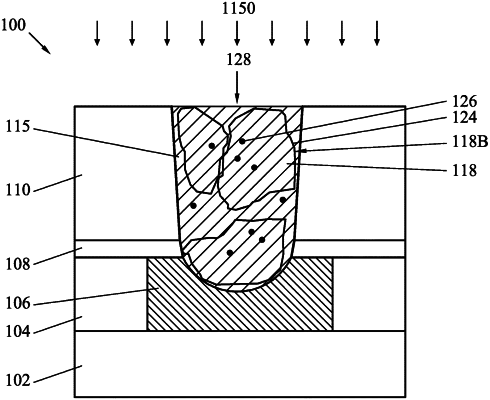
7. A semiconductor device structure, comprising:
a first dielectric layer over a substrate;
a first conductive feature in the first dielectric layer;
a second dielectric layer over the first dielectric layer and the first conductive feature; and
an electrical connection structure in the second dielectric layer and on the first conductive feature, wherein the electrical connection structure includes a second conductive feature made of a first metal material and a first inhibition layer in the second conductive feature and made of a second metal material, the first metal material is different than the second metal material, an interface between the second metal material and the first metal material is lower than a top surface of the second conductive feature and spaced apart from the top surface of the second conductive feature.
|
|
14. A semiconductor device structure, comprising:
a source/drain feature over a substrate;
a contact over the source/drain feature;
a dielectric layer over the contact;
a via through the dielectric layer and over the contact, wherein the via comprises a plurality of grains; and
an inhibition layer along grain boundaries of the grains of the via, wherein a first material of the via is different than a second material of the inhibition layer, and the inhibition layer includes a first portion laterally sandwiched between a first grain and a second grain of the plurality of grains and a second portion vertically sandwiched between the first grain and a third grain of the plurality of grains.
|