| CPC H01L 21/823431 (2013.01) [H01L 21/0217 (2013.01); H01L 21/02156 (2013.01); H01L 21/31111 (2013.01); H01L 21/823418 (2013.01); H01L 21/823437 (2013.01); H01L 21/823481 (2013.01); H01L 27/0886 (2013.01); H01L 29/0649 (2013.01); H01L 29/0847 (2013.01); H01L 29/66545 (2013.01); H01L 21/0274 (2013.01); H01L 21/26513 (2013.01); H01L 21/31053 (2013.01); H01L 21/324 (2013.01); H01L 21/76224 (2013.01); H01L 29/6656 (2013.01)] | 20 Claims |
|
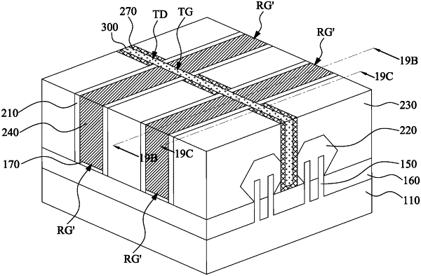
1. A device comprising:
a semiconductor fin over a substrate;
a gate structure over the semiconductor fin, wherein the gate structure comprises:
a gate dielectric layer over the semiconductor fin; and
a gate metal covering the gate dielectric layer;
gate spacers on opposite sides of the gate structure;
a dielectric feature over the substrate, wherein the dielectric feature is in contact with the gate metal, the gate dielectric layer, and the gate spacers, and an interface between the gate metal and the dielectric feature is substantially aligned with an interface between the dielectric feature and one of the gate spacers; and
an interlayer dielectric (ILD) layer laterally surrounding the gate structure, wherein the dielectric feature comprises:
a first portion in contact with the gate structure; and
a second portion embedded in the ILD layer, wherein a bottom surface of the first portion is lower than a bottom surface of the second portion.
|