| CPC H01L 21/823431 (2013.01) [H01L 21/02532 (2013.01); H01L 21/02603 (2013.01); H01L 21/823412 (2013.01); H01L 21/823418 (2013.01); H01L 21/823437 (2013.01); H01L 27/0886 (2013.01); H01L 29/0673 (2013.01); H01L 29/42392 (2013.01); H01L 29/66545 (2013.01); H01L 29/66553 (2013.01); H01L 29/66636 (2013.01); H01L 29/66742 (2013.01); H01L 29/78696 (2013.01); H01L 21/823807 (2013.01); H01L 21/823821 (2013.01)] | 20 Claims |
|
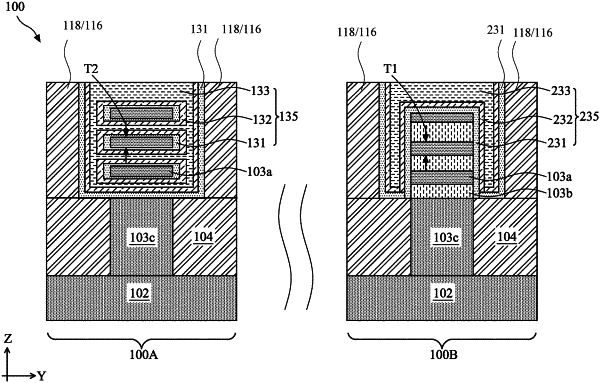
18. An integrated circuit (IC), comprising:
a substrate;
a first transistor on the substrate and in an IO area of the IC; and
a second transistor on the substrate and in a core area of the IC,
wherein the first transistor includes:
two first source/drain features,
a first fin base portion on the substrate,
a stack of first semiconductor layers and second semiconductor layers alternately stacked one over another, wherein the stack of the first and the second semiconductor layers are disposed vertically above the first fin base portion and laterally between the two first source/drain features, wherein the first and the second semiconductor layers include different materials,
a first gate dielectric layer disposed in direct contact with top and sidewalls of the stack of the first and the second semiconductor layers,
a first gate electrode layer disposed over the first gate dielectric layer, and
first dielectric spacers disposed laterally between each of the second semiconductor layers and each of the two first source/drain features,
wherein the first semiconductor layers directly interface with the two first source/drain features,
wherein the second transistor includes:
two second source/drain features,
a second fin base portion on the substrate,
a stack of third semiconductor layers above the second fin base portion and directly interfacing with the two second source/drain features,
a second gate dielectric layer wrapping around each of the third semiconductor layers,
a second gate electrode over the second gate dielectric layer, and
second dielectric spacers disposed laterally between the second gate dielectric layer and each of the two second source/drain features.
|