| CPC H01L 21/823412 (2013.01) [H01L 21/823431 (2013.01); H01L 21/823807 (2013.01); H01L 21/823821 (2013.01); H01L 29/0669 (2013.01); H01L 29/42392 (2013.01); H01L 29/66545 (2013.01); H01L 29/66553 (2013.01); H01L 29/775 (2013.01); H01L 29/785 (2013.01); H01L 29/78696 (2013.01)] | 20 Claims |
|
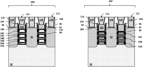
6. A transistor comprising:
a first nanostructure, the first nanostructure comprising first doped channel junctions at each end, the first nanostructure having a first undoped channel length between the first doped channel junctions;
a second nanostructure over the first nanostructure, the second nanostructure comprising second doped channel junctions at each end, the second nanostructure having a second undoped channel length between the second doped channel junctions, wherein a first lateral depth of the first doped channel junctions is a different value than a second lateral depth of the second doped channel junctions;
a third nanostructure, the third nanostructure interposed between the first nanostructure and the second nanostructure, the third nanostructure having a third undoped channel length between a first end of the third nanostructure and a second end of the third nanostructure, wherein each of the first nanostructure, second nanostructure, and third nanostructure have the same length, wherein the third undoped channel length is greater than or less than both the first undoped channel length and the second undoped channel length or wherein the third undoped channel length is the same as the first undoped channel length and the second undoped channel length is either greater than or less than the first undoped channel length;
a gate structure disposed over the first nanostructure and the second nanostructure, the gate structure wrapping around the first nanostructure and the second nanostructure; and
a first epitaxial region adjacent the gate structure, the first epitaxial region contacting the first nanostructure and the second nanostructure.
|