| CPC H01L 21/76897 (2013.01) [H01L 21/02123 (2013.01); H01L 21/02269 (2013.01); H01L 21/02274 (2013.01); H01L 21/76802 (2013.01); H01L 21/76877 (2013.01); H01L 21/823821 (2013.01); H01L 21/823871 (2013.01); H01L 27/0924 (2013.01); H01L 29/66795 (2013.01); H01L 29/785 (2013.01)] | 20 Claims |
|
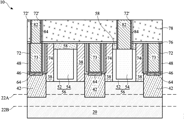
1. An integrated circuit structure comprising:
a dielectric layer;
a metal ring contacting sidewalls of the dielectric layer;
a metal region encircled by the metal ring; and
a silicon-and-nitrogen rich layer between the metal ring and the metal region, wherein a silicon atomic percentage in the silicon-and-nitrogen rich layer is higher than silicon atomic percentages in both of the metal ring and the metal region, and a first nitrogen atomic percentage in the silicon-and-nitrogen rich layer is higher than second nitrogen atomic percentages in the metal ring and the metal region.
|