| CPC H01L 21/76879 (2013.01) [C23C 16/00 (2013.01); C23C 16/045 (2013.01); C23C 16/50 (2013.01); H01L 21/28556 (2013.01); H01L 21/321 (2013.01); H01L 21/324 (2013.01); H01L 21/76856 (2013.01); H01L 21/76861 (2013.01); H01L 21/76876 (2013.01); H01L 21/76898 (2013.01); H10B 41/27 (2023.02); H10B 41/35 (2023.02); H01L 2924/0002 (2013.01)] | 18 Claims |
|
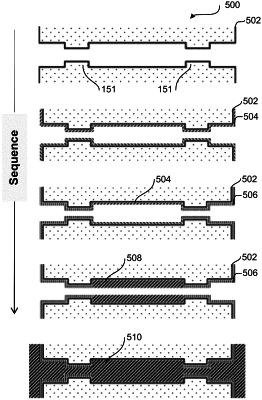
1. A method comprising:
providing a 3-D structure of a partially manufactured semiconductor substrate, the 3-D structure comprising sidewalls, a plurality of openings in the sidewalls leading to a plurality of features having a plurality of interior regions fluidically accessible through the openings, the plurality of interior regions comprising a tungsten layer deposited on a tungsten nucleation layer;
exposing the tungsten layer of the 3-D structure to diborane; and
after exposing the 3-D structure to diborane, exposing the 3-D structure to an inhibition chemistry to inhibit metal deposition on the tungsten layer.
|