| CPC H01L 21/76877 (2013.01) [H01L 21/3081 (2013.01); H01L 21/31138 (2013.01); H01L 21/7684 (2013.01); H01L 21/76802 (2013.01); H01L 21/76846 (2013.01); H01L 21/76847 (2013.01); H01L 21/76873 (2013.01)] | 20 Claims |
|
1. A method, comprising:
forming a photoresist comprising a bottom anti-reflective coating (BARC) material by introducing a conductive material into a photoresist polymer;
depositing, on a semiconductor substrate, the photoresist comprising the BARC material to form a photoresist layer;
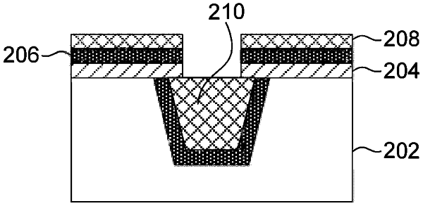
forming an opening in the photoresist layer and a portion of the semiconductor substrate;
depositing a conductive material in the opening and over the photoresist layer; and
planarizing the conductive material and the semiconductor substrate.
|